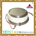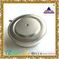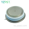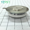
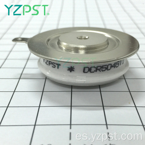

Semiconductor Devices DCR504 Power Thyristor
Obtener el último precio| Tipo de Pago: | L/C,T/T,Paypal |
| Incoterm: | FOB,CFR,CIF |
| transporte: | Ocean,Air |
| Hafen: | SHANGHAI |

| Tipo de Pago: | L/C,T/T,Paypal |
| Incoterm: | FOB,CFR,CIF |
| transporte: | Ocean,Air |
| Hafen: | SHANGHAI |
Modelo: YZPST-DCR504
Marca: YZPST
Control de fase de tiristor de alta potencia
YZPST-DCR504

|
Parameter |
Symbol |
Min. |
Max. |
Typ. |
Units |
Conditions |
|
Average value of on-state current |
IT(AV) |
|
300 |
|
A |
Sinewave,180o conduction,Tc=65oC |
|
RMS value of on-state current |
ITRMS |
|
480 |
|
A |
Nominal value |
|
Peak one cycle surge (non repetitive) current |
ITSM |
|
4200
4400 |
|
A
A |
8.3 msec (60Hz), sinusoidal wave- shape, 180o conduction, Tj = 125 oC 10.0 msec (50Hz), sinusoidal wave- shape, 180o conduction, Tj = 125 oC |
|
I square t |
I2t |
|
68000 |
|
A2s |
8.3 msec |
|
Latching current |
IL |
|
|
300 |
mA |
VD = 24 V; RL= 12 ohms |
|
Holding current |
IH |
|
|
200 |
mA |
VD = 24 V; I = 2.5 A |
|
Peak on-state voltage |
VTM |
|
2.98 |
|
V |
ITM = 1500 A; Tj = 25 oC |
|
Critical rate of rise of on-state current (5, 6) |
di/dt |
|
300 |
|
A/ms |
Switching from VDRM£ 1000 V, non-repetitive |
|
Critical rate of rise of on-state current (6) |
di/dt |
|
150 |
|
A/ms |
Switching from VDRM£ 1000 V |
CARACTERÍSTICAS ELÉCTRICAS Y CALIFICACIONES Gating Dynamic
|
Parameter |
Symbol |
Min. |
Max. |
Typ. |
Units |
Conditions |
|
Peak gate power dissipation |
PGM |
|
10 |
|
W |
tp = 40 us |
|
Average gate power dissipation |
PG(AV) |
|
2 |
|
W |
|
|
Peak gate current |
IGM |
|
3 |
|
A |
|
|
Gate current required to trigger all units |
IGT |
|
200 150 125 |
|
mA mA mA |
VD = 6 V;RL = 3 ohms;Tj = -40 oC VD = 6 V;RL = 3 ohms;Tj = +25 oC VD = 6 V;RL = 3 ohms;Tj = +125oC |
|
Gate voltage required to trigger all units
|
VGT |
0.30 |
3 2.5
|
|
V V V |
VD = 6 V;RL = 3 ohms;Tj = -40 oC VD = 6 V;RL = 3 ohms;Tj = 0-125oC VD = Rated VDRM; RL = 1000 ohms; Tj = + 125 oC |
|
Peak negative voltage |
VGRM |
|
5 |
|
V |
|
|
Parameter |
Symbol |
Min. |
Max. |
Typ. |
Units |
Conditions |
|
Delay time |
td |
|
1.0 |
|
ms |
ITM = 100 A; VD = VDRM Gate pulse: VG = 10 V; RG = 25 ohms; tr = 0.1 ms; tp = 20 ms |
|
Turn-off time (with VR = -50 V) |
tq |
|
200
|
|
ms |
ITM > 250 A; di/dt = 10 A/ms; VR³ -50 V; Re-applied dV/dt = 20 V/ms linear to VDRM ; Tj = 125 oC; Duty cycle ³ 0.01% |
|
Reverse recovery charge |
Qrrr |
|
200 |
|
mCb |
ITM > 400 A; di/dt = 10 A/ms; |
CARACTERÍSTICAS TÉRMICAS Y MECÁNICAS Y CALIFICACIONES
|
Parameter |
Symbol |
Min. |
Max. |
Typ. |
Units |
Conditions |
|
Operating temperature |
Tj |
-40 |
+125 |
|
oC |
|
|
Storage temperature |
Tstg |
-40 |
+150 |
|
oC |
|
|
Thermal resistance - junction to case |
RQ (j-c) |
|
0.095 |
|
oC/W |
Double sided cooled |
|
Thermal resistamce - case to sink |
RQ (c-s) |
|
0.06 |
|
oC/W |
Double sided cooled * |
|
Mounting force |
P |
3.2 |
3.9 |
|
kN |
|
|
Weight |
W |
|
|
57 |
g. |
|
* Superficies de montaje lisas, planas y engrasadas
Nota: para el contorno y las dimensiones del caso, consulte el dibujo del esquema del caso en la última página de esta Información técnica
RESUMEN Y DIMENSIONES DEL CASO.


Número de Teléfono: 86-514-87782298
Whatsapp: +8613805278321
Dirección: 3rd Floor, Weiheng Building No.20 B Area, Yangzhou, Jiangsu China
Sitio Web: https://es.yzpst.com


Privacy statement: Your privacy is very important to Us. Our company promises not to disclose your personal information to any external company with out your explicit permission.
Fill in more information so that we can get in touch with you faster
Privacy statement: Your privacy is very important to Us. Our company promises not to disclose your personal information to any external company with out your explicit permission.