

Encendedor electronico 30V Mosfet 80N03
$0.23≥1000Piece/Pieces
| Tipo de Pago: | L/C,T/T,Paypal |
| Incoterm: | FOB,CFR,CIF |
| Cantidad de pedido mínima: | 1000 Piece/Pieces |
| transporte: | Ocean,Air |
| Hafen: | Shanghai |

$0.23≥1000Piece/Pieces
| Tipo de Pago: | L/C,T/T,Paypal |
| Incoterm: | FOB,CFR,CIF |
| Cantidad de pedido mínima: | 1000 Piece/Pieces |
| transporte: | Ocean,Air |
| Hafen: | Shanghai |
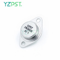
Modelo: YZPST-80N03
Marca: YZPST
| Unidades de venta | : | Piece/Pieces |
| Tipo de paquete | : | 1. Embalaje anti-electrostático 2. Caja de cartón 3. Embalaje protector de plástico |
Encendedor de cigarrillos electronico Mosfet
YZPST-80N03
|
VDSS 30V RDS(ON) 4mΩ(max.)@ VGS=10V RDS(ON) 6mΩ(max.)@ VGS=4.5V ID 100A |
|
|
Description |
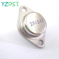
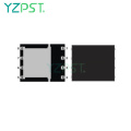
DFN5X6-8L |
|
YZPST 80N03 uses advanced Trench technology and designs to provide excellent RDS(ON) with low gate charge. This device is suitable for use in PWM, load switching and general purpose applications. |
|
|
Applications |
Features |
|
■ Lithium-Ion Secondary Batteries ■ Load Switch ■ DC-DC converters and Off-line UPS |
■ Low On-Resistance ■ Low Input Capacitance ■ Low Miller Charge ■ Low Input / Output Leakage |
|
Absolute Maximum Ratings (TA=25°C unless otherwise noted) |
|||
|
Parameter |
Symbol |
Value |
Unit |
|
Drain-Source Voltage |
VDSS |
30V |
V |
|
Gate-Source Voltage |
VGSS |
±20V |
V |
|
Drain Current-Continuous @ TC=25℃ NOTE1, 6 |
ID |
100 |
A |
|
Drain Current-Continuous @ TC=100℃ NOTE1, 6 |
80 |
A |
|
|
Drain Current-Continuous @ TA=25℃ NOTE1 |
ID |
20 |
A |
|
Drain Current-Continuous @ TA=100℃ NOTE1 |
15 |
A |
|
|
Drain Current-Pulsed NOTE 2 |
IDM |
216 |
A |
|
Avalanche Current |
IAS |
53.8 |
A |
|
Avalanche Energy NOTE 3 |
EAS |
144.7 |
mJ |
|
Maximum Power Dissipation @ TC=25℃ NOTE4 |
PD |
69 |
W |
|
Maximum Power Dissipation @ TA=25℃ NOTE4 |
2 |
W |
|
|
Storage Temperature Range |
TSTG |
-55 to 150°C |
°C |
|
Operating Junction Temperature Range |
TJ |
-55 to 150°C |
°C |
|
Thermal Resistance Ratings |
||||||
|
Parameter |
Symbol |
Conditions |
Min. |
Typ. |
Max. |
Unit |
|
Maximum Junction-to-Ambient NOTE1 |
RθJA |
Steady State |
- |
- |
62 |
°C/W |
|
Maximum Junction-to-Case NOTE1 |
RθJC |
Steady State |
- |
- |
1.8 |
°C/W |
|
Electrical Characteristics(TJ=25°C unless otherwise noted) |
||||||
|
Parameter |
Symbol |
Conditions |
Min. |
Typ. |
Max. |
Unit |
|
OFF CHARACTERISTICS |
||||||
|
Drain-Source Breakdown Voltage |
BVDSS |
VGS=0V , IDS=250uA |
30 |
- |
- |
V |
|
Zero Gate Voltage Drain Current |
IDSS |
VDS=24V, VGS=0V |
- |
- |
1 |
uA |
|
Gate-Source Leakage Current |
IGSS |
VGS=±20V , VDS=0V |
- |
- |
±100 |
nA |
|
ON CHARACTERISTICS |
||||||
|
Gate Threshold Voltage |
VGS(TH) |
VGS=VDS, IDS=250uA |
1.2 |
- |
2.5 |
V |
|
Drain-Source On-Resistance NOTE2 |
RDS(ON) |
VGS=10V , IDS=30A |
- |
- |
4 |
mΩ |
|
VGS=4.5V , IDS=20A |
- |
- |
6 |
mΩ |
||
|
Forward Transconductance |
gfs |
VDS=5V , ID=30A |
- |
26.5 |
- |
S |
|
Gate Resistance |
Rg |
VDS=0V , VGS=0V , f=1MHz |
- |
1.4 |
- |
Ω |
|
DYNAMIC CHARACTERISTICS |
||||||
|
Input Capacitance |
Ciss |
VDS=15V, VGS=0V, f=1MHz |
- |
3080 |
- |
pF |
|
Output Capacitance |
Coss |
- |
410 |
- |
||
|
Reverse Transfer Capacitance |
Crss |
- |
316 |
- |
||
|
SWITCHING CHARACTERISTICS |
||||||
|
Turn-On Delay Time |
Td(on) |
VDS=15V, VGS=10V, ID=15A , RGEM=3.3Ω |
- |
9.6 |
- |
ns |
|
Rise Time |
tr |
- |
20.8 |
- |
||
|
Turn-Off Delay Time |
Td(off) |
- |
58 |
- |
||
|
Fall Time |
tf |
- |
16 |
- |
||
|
Total Gate Charge at 4.5V |
Qg |
VDS=15V, IDS=15A, VGS=4.5V |
- |
32 |
- |
nC |
|
Gate to Source Gate Charge |
Qgs |
- |
9.1 |
- |
||
|
Gate to Drain "Miller" Charge |
Qgd |
- |
12.2 |
- |
||
|
SWITCHING CHARACTERISTICS |
||||||
|
Drain-Source Diode Forward Voltage 2 |
VSD |
VGS=0V, IS=1A |
- |
- |
1.0 |
V |
|
Continuous Source Current NOTE1, 5 |
IS |
VG=VD=0V , Force Current |
- |
- |
100 |
A |
|
Pulsed Source Current NOTE2,5 |
ISM |
- |
- |
216 |
A |
|
Notas:
1. Los datos probados por superficie montados en una placa FR-4 de 1 pulgada2 con cobre 2OZ.
2. Los datos probados por pulsos, ancho de pulso ≦ 300us, ciclo de trabajo ≦ 2%
3. Los datos de EAS muestran Max. clasificación. La condición de prueba es VDD = 25V, VGS = 10V, L = 0.1mH, IAS = 53.8A
4. La disipación de potencia está limitada por una temperatura de unión de 175
5. Los datos son teóricamente los mismos que ID y IDM, en aplicaciones reales, deben estar limitados por la disipación total de potencia.
6. La limitación actual del paquete es de 85A.W. Disipación.
")
")
")
")


Número de Teléfono: 86-514-87782298
Whatsapp: +8613805278321
Dirección: 3rd Floor, Weiheng Building No.20 B Area, Yangzhou, Jiangsu China
Sitio Web: https://es.yzpst.com


Privacy statement: Your privacy is very important to Us. Our company promises not to disclose your personal information to any external company with out your explicit permission.
Fill in more information so that we can get in touch with you faster
Privacy statement: Your privacy is very important to Us. Our company promises not to disclose your personal information to any external company with out your explicit permission.