Tiristores de encapsulación de potencia de alta frecuencia DC
Obtener el último precio| Tipo de Pago: | L/C,T/T,Paypal |
| Incoterm: | FOB,CFR,CIF |
| transporte: | Ocean,Air |
| Hafen: | Shanghai |

| Tipo de Pago: | L/C,T/T,Paypal |
| Incoterm: | FOB,CFR,CIF |
| transporte: | Ocean,Air |
| Hafen: | Shanghai |
Modelo: YZPST-T700123503BY
Marca: Yzpst
| Unidades de venta | : | Others |
| Descargar | : |
|
Tiristores de control de fase
YZPST-T700123503by
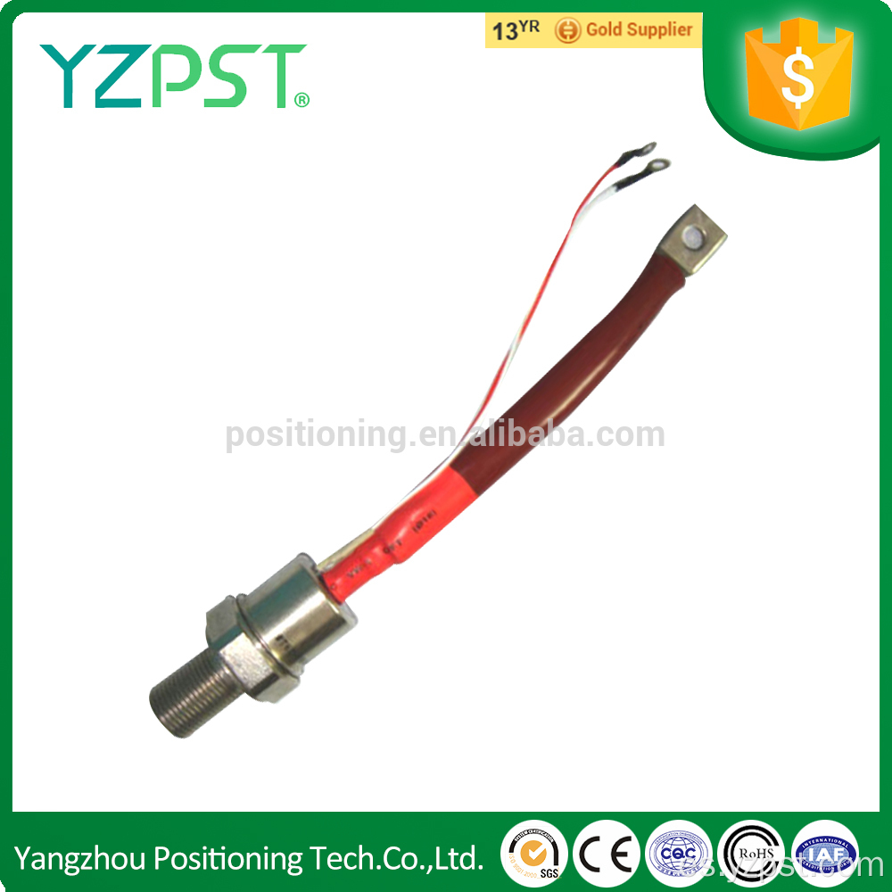
Características de los tiristores de control de fase: configuración de la puerta de amplificación central, encapsulación unida por compresión, alta capacidad de DV/DT y tipo de perno, pulgada de rosca o métrica. Las aplicaciones típicas de los tiristores de alta frecuencia son la conmutación de alimentación media y las alimentaciones de CC.
Calificaciones y características máximas
|
Symbol |
Parameter |
Values |
Units |
Test Conditions |
|
|
ON-STATE |
|
|
|
||
|
ITAV |
Mean on-state current |
350 |
A |
Sinewave,180° conduction,Tc=85℃ |
|
|
ITRMS |
RMS value of on-state current |
550 |
A |
Nominal value |
|
|
ITSM |
Peak one cycle surge (non repetitive) current |
9.1 |
KA |
10.0 msec (50Hz), sinusoidal wave- shape, 180o conduction, Tj = 125 oC |
|
|
I2t |
I square t |
416 |
KA2s |
8.3 msec and 10.0 msec |
|
|
IL |
Latching current |
- |
mA |
VD = 24 V; RL= 12 ohms |
|
|
IH |
Holding current |
- |
mA |
VD = 24 V; I = 2.5 A |
|
|
VTM |
Peak on-state voltage |
1.4 |
V |
ITM = 625 A; Duty cycle £ 0.01%
|
|
|
di/dt |
Critical rate of rise of on-state current |
non-repetitive |
800 |
A/ms |
Gate drive 20V, 20Ω, tr≤1μs, Tj=Tjmax, anode voltage≤80% VDRM |
|
repetitive |
150 |
||||
|
BLOCKING |
|
|
|
||
|
VDRM VRRM |
Repetitive peak off state voltage Repetitive peak reverse voltage |
1200 |
V |
|
|
|
VDSM VRSM |
Non repetitive peak off state voltage Non repetitive peak reverse voltage |
1300 |
V |
|
|
|
IDRM IRRM |
Repetitive peak off state current Repetitive peak reverse current |
30 |
mA |
Tj = 125 oC ,VRRM VDRM applied |
|
|
dV/dt |
Critical rate of voltage rise |
1000 |
V/ms |
TJ=TJmax, linear to 80% rated VDRM |
|
|
TRIGGEING |
|
|
|
||
|
PG(AV) |
Average gate power dissipation |
3 |
W |
|
|
|
PGM |
Peak gate power dissipation |
16 |
W |
|
|
|
IGM |
Peak gate current |
- |
A |
|
|
|
IGT |
Gate trigger current |
150 |
mA |
TC = 25 oC |
|
|
VGT |
Gate trigger voltage |
3.0 |
V |
TC = 25 oC |
|
|
VGD |
Gate non-trigger voltage |
0.15 |
V |
Tj = 125 oC |
|
|
SWITCHING |
|
|
|
||
|
tq |
Turn-off time |
150 |
ms |
ITM=550A, TJ=TJmax, di/dt=40A/μs, VR=50V, dv/dt=20V/μs, Gate 0V 100Ω, tp=500μs |
|
|
td |
Delay time |
- |
|
Gate current A, di/dt=40A/μs, Vd=0.67%VDRM, TJ=25 oC |
|
Qrr |
Reverse recovery charge |
- |
|
|
Térmico y mecánico
|
Symbol |
Parameter |
Values |
Units |
Test Conditions |
|
Tj |
Operating temperature |
-40~125 |
oC |
|
|
Tstg |
Storage temperature |
-40~150 |
oC |
|
|
R th (j-c) |
Thermal resistance - junction to case |
0.1 |
oC/W |
DC operation ,Single sided cooled |
|
R th (c-s) |
Thermal resistance - case to sink |
0.05 |
oC/W |
Single sided cooled |
|
P |
Mounting force |
3.5 |
Nm |
|
|
W |
Weight |
- |
g |
about |


Número de Teléfono: 86-514-87782298
Whatsapp: +8613805278321
Dirección: 3rd Floor, Weiheng Building No.20 B Area, Yangzhou, Jiangsu China
Sitio Web: https://es.yzpst.com


Privacy statement: Your privacy is very important to Us. Our company promises not to disclose your personal information to any external company with out your explicit permission.
Fill in more information so that we can get in touch with you faster
Privacy statement: Your privacy is very important to Us. Our company promises not to disclose your personal information to any external company with out your explicit permission.