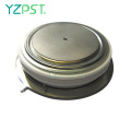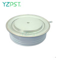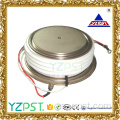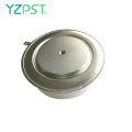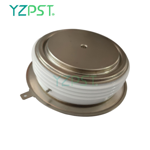
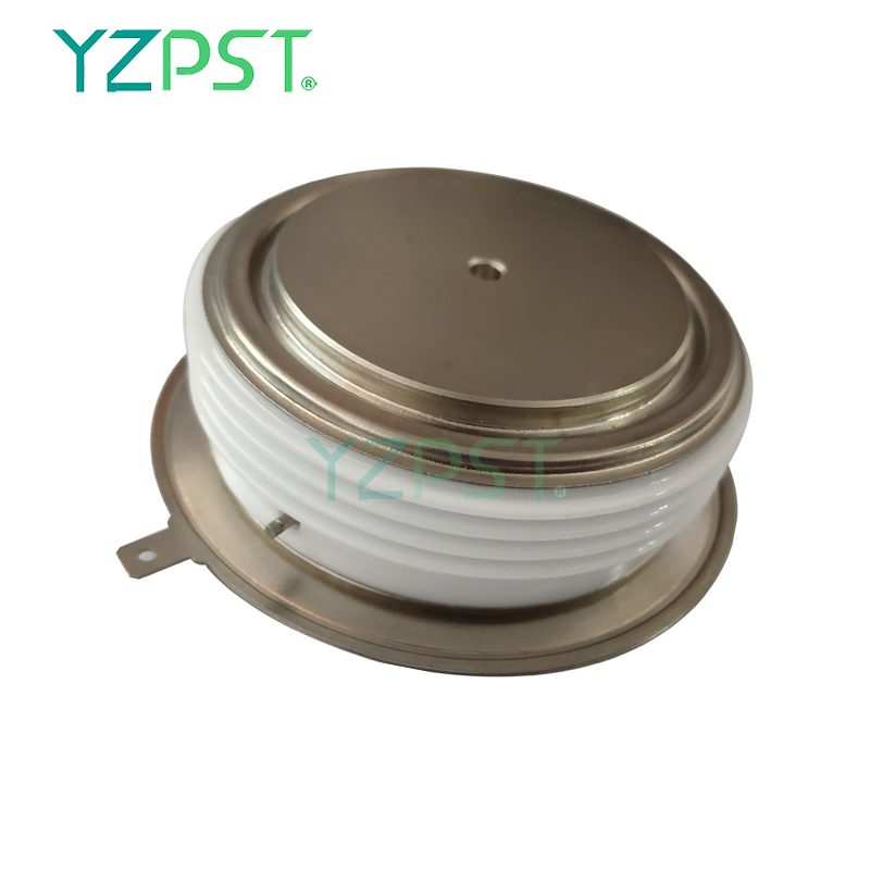
Tiristor promocional de alta potencia para control de fase
Obtener el último precio| Tipo de Pago: | L/C,T/T,Paypal |
| Incoterm: | FOB,CFR,CIF |
| transporte: | Ocean,Air |
| Hafen: | Shanghai |

| Tipo de Pago: | L/C,T/T,Paypal |
| Incoterm: | FOB,CFR,CIF |
| transporte: | Ocean,Air |
| Hafen: | Shanghai |
Modelo: YZPST-R219CH12FN0
Marca: YZPST
Tiristor de alta potencia para control de fase
YZPST-R219CH12FN0
caracteristicas:
Tiempo de apagado máximo garantizado.
. Toda estructura difusa
. Dispositivo ensamblado a presión
Configuración de compuerta amplificadora interdigitada
. Alta capacidad dV / dt
CARACTERÍSTICAS ELÉCTRICAS Y CLASIFICACIONES
Bloqueo - Estado desactivado
|
|
|
VRRM (1) |
VDRM (1) |
VRSM (1) |
|
1200 |
1200 |
1300 |
V RRM = Voltaje inverso pico repetitivo
V DRM = Voltaje repetitivo de estado pico apagado
V RSM = Tensión inversa pico no repetitiva (2)
|
Repetitive peak reverse leakage and off state leakage |
IRRM / IDRM |
15 mA 70 mA (3) |
|
Critical rate of voltage rise |
dV/dt (4) |
200 V/msec |
Notas:
Todas las clasificaciones se especifican para Tj = 25 o C a menos que se indique lo contrario.
(1) Todas las clasificaciones de voltaje se especifican para un
Forma de onda sinusoidal de 50Hz / 60zHz sobre el
rango de temperatura -40 a +125 o C.
(2) 10 ms. max. ancho de pulso
(3) Valor máximo para Tj = 125 o C.
(4) Valor mínimo para forma de onda lineal y exponencial a 80% de V DRM nominal. Puerta abierta. Tj = 125 o C.
(5) Valor no repetitivo.
(6) El valor de di / dt se establece de acuerdo con el estándar EIA / NIMA RS-397, Sección 5-2-2-6. El valor definido sería adicional al obtenido de un circuito ubber, que comprende un condensador de 0.2 m F y una resistencia de 20 ohmios en paralelo con el thristor bajo prueba.
Conducción - en estado
|
Parameter |
Symbol |
Min. |
Max. |
Typ. |
Units |
Conditions |
|
Max. average value of on-state current |
IT(AV)M |
|
929 |
|
A |
Sinewave,180o conduction,Tc=55oC |
|
RMS value of on-state current |
IT(RMS)m |
|
1893 |
|
A |
Nominal value |
|
Peak one cPSTCle surge (non repetitive) current |
ITSM |
|
-
9.0 |
|
kA
kA |
8.3 msec (60Hz), sinusoidal wave- shape, 180o conduction, Tj = 125 oC 10.0 msec (50Hz), sinusoidal wave- shape, 180o conduction, Tj = 125 oC |
|
I square t |
I2t |
|
405x103 |
|
A2s |
8.3 msec |
|
Latching current |
IL |
|
- |
|
mA |
VD = 24 V; RL= 12 ohms |
|
Holding current |
IH |
|
1000 |
|
mA |
VD = 24 V; I = 2.5 A |
|
Peak on-state voltage |
VTM |
|
2.04 |
|
V |
ITM = 1400 A |
|
Critical rate of rise of on-state current (5, 6) |
di/dt |
|
1500 |
|
A/ms |
Switching from VDRM £ 1000 V, non-repetitive |
|
Critical rate of rise of on-state current (6) |
di/dt |
|
1000 |
|
A/ms |
Switching from VDRM £ 1000 V |
Gating
|
Parameter |
Symbol |
Min. |
Max. |
Typ. |
Units |
Conditions |
|
Peak gate power dissipation |
PGM |
|
30 |
|
W |
|
|
Average gate power dissipation |
PG(AV) |
|
2 |
|
W |
|
|
Peak gate current |
IGM |
|
- |
|
A |
|
|
Gate current required to trigger all units |
IGT |
|
300 |
|
mA |
VD = 10 V;IT=3A;Tj = +25 oC
|
|
Gate voltage required to trigger all units
|
VGT |
|
3.0 |
|
V
|
VD = 10 V;IT=3A;Tj = +25 oC
|
|
Peak negative voltage |
VRGM |
|
5 |
|
V |
|
Dinámica
|
Parameter |
Symbol |
Min. |
Max. |
Typ. |
Units |
Conditions |
|
Delay time |
tgd |
|
1.0 |
- |
ms |
VD=67% VDRM, IT=2000A, di/dt=60A/us, IFG=2A, tr=0.5us, Tj=25C |
|
Turn-on time |
tgt |
|
2.0 |
- |
|
|
|
Turn-off time (with VR = -5 V) |
tq |
- |
- |
10 |
ms |
ITM=1000A, tp=1000us, di/dt=60A/us, Vr=50V, Vdr=33%VDRM, dVdr/dt=200V/us |
|
Reverse recovery current |
Irm |
|
- |
|
A |
ITM=4000A, tp=2000us, di/dt=60A/us |


Número de Teléfono: 86-514-87782298
Whatsapp: +8613805278321
Dirección: 3rd Floor, Weiheng Building No.20 B Area, Yangzhou, Jiangsu China
Sitio Web: https://es.yzpst.com


Privacy statement: Your privacy is very important to Us. Our company promises not to disclose your personal information to any external company with out your explicit permission.
Fill in more information so that we can get in touch with you faster
Privacy statement: Your privacy is very important to Us. Our company promises not to disclose your personal information to any external company with out your explicit permission.