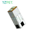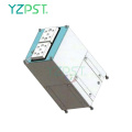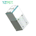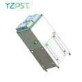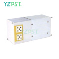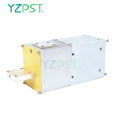
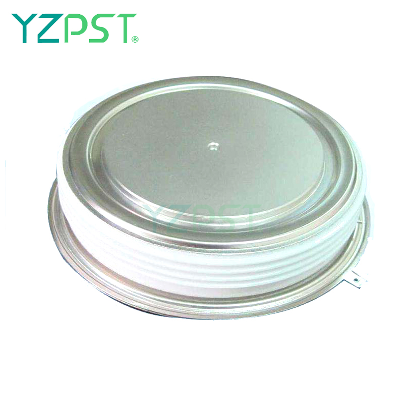
Tiristor inversor de alta potencia C458PB
Obtener el último precio| Tipo de Pago: | L/C,T/T,Paypal |
| Incoterm: | FOB,CFR,CIF |
| transporte: | Ocean,Air |
| Hafen: | SHANGHAI |

| Tipo de Pago: | L/C,T/T,Paypal |
| Incoterm: | FOB,CFR,CIF |
| transporte: | Ocean,Air |
| Hafen: | SHANGHAI |
Modelo: YZPST-C458PB
Marca: YZPST
| Tipo de paquete | : | 1. Embalaje anti-electrostático 2. Caja de cartón 3. Embalaje protector de plástico |
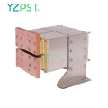
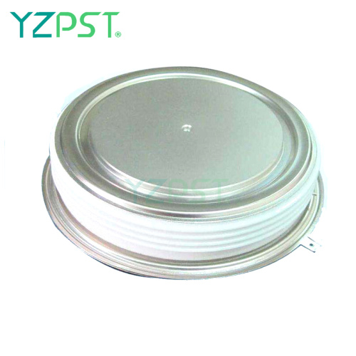
Tiristor de alta potencia
YZPST-DCR1020SF65-1
Aplicación de tiristores Control de tiristores de motor de CC Tiristor de dispositivo ensamblado a presión Todas las clasificaciones se especifican para Tj = 25 oC a menos que se indique lo contrario.
(1) Todas las clasificaciones de voltaje se especifican para una forma de onda sinusoidal aplicada de 50Hz / 60zHz en el rango de temperatura de -40 a +125 oC.
(2) 10 ms. max. ancho de pulso
(3) Valor máximo para Tj = 125 oC.
(4) Valor mínimo para forma de onda lineal y exponencial a 80% de VDRM nominal. Puerta abierta. Tj = 125 oC.
(5) Valor no repetitivo.
(6) El valor de di / dt se establece de acuerdo con la Norma EIA / NIMA RS-397, Sección 5-2-2-6. El valor definido sería adicional
ción a la obtenida de un circuito amortiguador, que comprende un condensador de 0.2 F y una resistencia de 20 ohmios en paralelo con el thristor bajo prueba.
Características:. Toda estructura difusa . Configuración de compuerta de amplificación central . Capacidad de bloqueo de hasta 4200 voltios
. Máximo tiempo de apagado garantizado . Alta capacidad dV / dt . Dispositivo ensamblado a presión

|
Parameter |
Symbol |
Min. |
Max. |
Typ. |
Units |
Conditions |
|
Average value of on-state current |
IT(AV) |
|
640 |
|
A |
Sinewave,180o conduction,T =60oC c |
|
RMS value of on-state current |
ITRMS |
|
1005 |
|
A |
Nominal value |
|
Peak one cPSTCle surge (non repetitive) current |
ITSM |
|
-
8.5 |
|
KA KA |
8.3 msec (60Hz), sinusoidal wave- shape, 180o conduction, T = 125 j oC 10.0 msec (50Hz), sinusoidal wave- shape, 180o conduction, T = 125 j oC |
|
I square t |
I2t |
|
0.36x10⁶ |
|
A2s |
8.3 msec and 10.0 msec |
|
Latching current |
IL |
|
600 |
|
mA |
VD = 24 V; RL= 12 ohms |
|
Holding current |
IH |
|
200 |
|
mA |
VD = 24 V; I = 2.5 A |
|
Peak on-state voltage |
VTM |
|
3.6 |
|
V |
ITM = 1800 A; Duty cPSTCle 0.01%; T = 25 oC j |
|
Critical rate of rise of on-state current (5, 6) |
di/dt |
|
- |
|
A/ s |
Switching from VDRM 1000 V, non-repetitive |
|
Critical rate of rise of on-state current (6) |
di/dt |
|
100 |
|
A/ s |
Switching from VDRM 1000 V |
E L E CTR I C A L CH A R A C T E R IS T I C S A N D R A T I N G S
|
G a t i n g
|
Parameter |
Symbol |
Min. |
Max. |
Typ. |
Units |
Conditions |
|
Peak gate power dissipation |
PGM |
|
150 |
|
W |
tp = 40 us |
|
Average gate power dissipation |
PG(AV) |
|
5 |
|
W |
|
|
Peak gate current |
IGM |
|
- |
|
A |
|
|
Gate current required to trigger all units |
IGT |
|
- 300 - |
|
mA mA mA |
V = 6 V;R = 3 ohms;T = -40 oC D L j V = 6 V;R = 3 ohms;T = +25 oC D L j V = 6 V;R = 3 ohms;T = +125oC D L j |
|
Gate voltage required to trigger all units |
V |
|
- 3.0 - |
|
V V V |
V = 6 V;R = 3 ohms;T = -40 oC D L j V = 6 V;R = 3 ohms;T = 0-125oC D L j VD = Rated VDRM; RL = 1000 ohms; T = + 125 oC j |
|
Peak negative voltage |
VGRM |
|
5 |
|
V |
|
D y n a m i c
|
Parameter |
Symbol |
Min. |
Max. |
Typ. |
Units |
Conditions |
|
Delay time |
td |
|
- |
0.5 |
s |
ITM = 50 A; VD = Rated VDRM Gate pulse: VG = 20 V; RG = 20 ohms; tr = 0.1 s; tp = 20 s |
|
Turn-off time (with VR = -50 V) |
tq |
|
- |
600 |
s |
ITM = 1000 A; di/dt = 25 A/ s; VR -50 V; Re-applied dV/dt = 20 V/ s linear to 80% VDRM; VG = 0; T = 125 oC; Duty cPSTCle j 0.01% |
|
Reverse recovery charge |
Qrr |
|
* |
|
C |
ITM = 1000 A; di/dt = 25 A/ s; VR -50 V |
* * F o r gu a r a n t eed m a x . v a lu e , c on t a c t f a c t o r y .
T H E R M A L A N D ME CH A N I C A L CH A R A C T E R IS T I C S A N D R A T I N G S
|
Parameter |
Symbol |
Min. |
Max. |
Typ. |
Units |
Conditions |
|
Operating temperature |
Tj |
-40 |
+125 |
|
oC |
|
|
Storage temperature |
Tstg |
-40 |
+125 |
|
oC |
|
|
Thermal resistance - junction to case |
R (j-c) |
|
0.022 0.052 |
|
o C/W |
Double sided cooled Single sided cooled |
|
Thermal resistamce - case to sink |
R (c-s) |
|
0.004 0.008 |
|
o C/W |
Double sided cooled * Single sided cooled * |
|
Thermal resistamce - junction to sink |
R (j-s) |
|
- - |
|
o C/W |
Double sided cooled * Single sided cooled * |
|
Mounting force |
P |
18 |
22 |
|
kN |
|
|
Weight |
W |
|
|
- |
g |
|
* * M ou n t i ng s ur f a c es s m oo t h, f l a t y g r e a s ed
RESUMEN DEL CASO Y DIMENSIONES


Número de Teléfono: 86-514-87782298
Whatsapp: +8613805278321
Dirección: 3rd Floor, Weiheng Building No.20 B Area, Yangzhou, Jiangsu China
Sitio Web: https://es.yzpst.com


Privacy statement: Your privacy is very important to Us. Our company promises not to disclose your personal information to any external company with out your explicit permission.
Fill in more information so that we can get in touch with you faster
Privacy statement: Your privacy is very important to Us. Our company promises not to disclose your personal information to any external company with out your explicit permission.